Q1GATE 2025MSQ
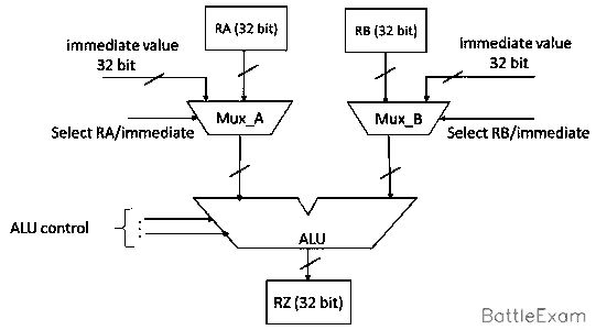
A partial data path of a processor is given in the figure, where , , and are 32-bit registers. Which option(s) is/are CORRECT related to arithmetic operations using the data path as shown?
GATE CSE · Computer Organization Architecture
Master topic for ALU Data Path and Control Unit. Includes Number Representation, Boolean Algebra & Logic Gates.
97 questions · 20 PYQs · 0 AI practice · GATE CSE 2027
🎯 These are sample questions
Just sign in to unlock everything. Free for all students.
A partial data path of a processor is given in the figure, where , , and are 32-bit registers. Which option(s) is/are CORRECT related to arithmetic operations using the data path as shown?
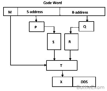
Consider a digital display system (DDS) shown in the figure that displays the contents of register X. A 16-bit code word is used to load a word in X, either from S or from R. S is a 1024-word memory segment and R is a 32-word register file. Based on the value of mode bit M, T selects an input word to load in X. P and Q interface with the corresponding bits in the code word to choose the addressed word. Which one of the following represents the functionality of P, Q, and T?
Micro program is:
Consider a main memory system that consists of 8 memory modules attached to the system bus, which is one word wide. When a write request is made, the bus is occupied for 100 nanoseconds (ns) by the data, address, and control signals. During the same 100 ns, and for 500 ns thereafter, the addressed memory module executes one cycle accepting and storing the data. The (internal) operation of different memory modules may overlap in time, but only one request can be on the bus at any time. The maximum number of stores (of one word each) that can be initiated in 1 millisecond is ____________
Two control signals in microprocessor which are related to Direct Memory Access (DMA) are
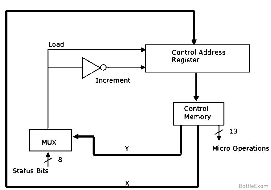
The microinstructions stored in the control memory of a processor have a width of 26 bits. Each microinstruction is divided into three fields. a micro operation field of 13 bits, a next address field (X), and a MUX select field (Y). There are 8 status bits in the inputs of the MUX. How many bits are there in the X and Y fields, and what is the size of the control memory in number of words?
Consider a CPU where all the instructions require 7 clock cycles to complete execution. There are 140 instructions in the instruction set. It is found that 125 control signals are needed to be generated by the control unit. While designing the horizontal microprogrammed control unit, single address field format is used for branch control logic. What is the minimum size of the control word and control address register?
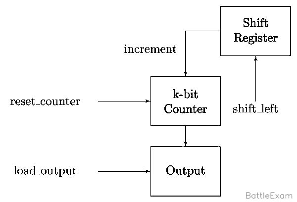
The data path shown in the figure computes the number of 1s in the 32-bit input word corresponding to an unsigned even integer stored in the shift register. The unsigned counter, initially zero, is incremented if the most significant bit of the shift register is 1. The microprogram for the control is shown in the table below with missing control words for microinstructions .
The counter width (k), the number of missing microinstructions (n), and the control word for microinstructions are, respectively,
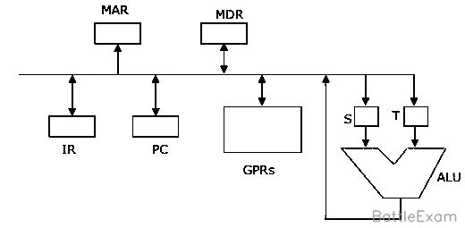
Consider the following data path of a CPU. ALU, the bus and all the registers in the data path are of identical size. All operations including incrementation of the PC and the GPRs are to be carried out in the ALU. Two clock cycles are needed for memory read operation - the first one for loading address in the MAR and the next one for loading data from the memory bus into the MDR. The instruction "call Rn, sub" is a two word instruction. Assuming that PC is incremented during the fetch cycle of the first word of the instruction, its register transfer interpretation is Rn < = PC + 1; PC < = M[PC]; The minimum number of CPU clock cycles needed during the execution cycle of this instruction is:
An instruction set of a processor has 125 signals which can be divided into 5 groups of mutually exclusive signals as follows: Group 1 : 20 signals, Group 2 : 70 signals, Group 3 : 2 signals, Group 4 : 10 signals, Group 5 : 23 signals. How many bits of the control words can be saved by using vertical microprogramming over horizontal microprogramming?
A hardwired CPU uses 10 control signals to , in various time steps to , to implement 4 instructions to as shown below:
Which of the following pairs of expressions represent the circuit for generating control signals and respectively? indicates that the control signal should be generated in time step if the instruction being executed is or )
Consider the following data path of a CPU. ALU, the bus and all the registers in the data path are of identical size. All operations including incrementation of the PC and the GPRs are to be carried out in the ALU. Two clock cycles are needed for memory read operation - the first one for loading address in the MAR and the next one for loading data from the memory bus into the MDR. The instruction "add R0, R1" has the register transfer interpretation R0<=R0+R1. The minimum number of clock cycles needed for execution cycle of this instruction is.
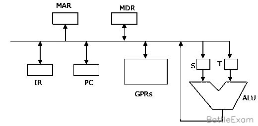
Consider a three word machine instruction ADD A[R0], @B The first operand (destination) "A[R0]" uses indexed addressing mode with R0 as the index register. The second operand (source) "@B" uses indirect addressing mode. A and B are memory addresses residing at the second and the third words, respectively. The first word of the instruction specifies the opcode, the index register designation and the source and destination addressing modes. During execution of ADD instruction, the two operands are added and stored in the destination (first operand). The number of memory cycles needed during the execution cycle of the instruction is:
The microinstructions stored in the control memory of a processor have a width of 26 bits. Each microinstruction is divided into three fields: a micro-operation field of 13 bits, a next address field (X), and a MUX select field (Y). There are 8 status bits in the inputs of the MUX. How many bits are there in the X and Y fields, and what is the size of the control memory in number of words?
A CPU has only three instructions I1, I2 and I3, which use the following signals in time steps T1-T5: I1 : T1 : Ain, Bout, Cin T2 : PCout, Bin T3 : Zout, Ain T4 : Bin, Cout T5 : End I2 : T1 : Cin, Bout, Din T2 : Aout, Bin T3 : Zout, Ain T4 : Bin, Cout T5 : End I3 : T1 : Din, Aout T2 : Ain, Bout T3 : Zout, Ain T4 : Dout, Ain T5 : End Which of the following logic functions will generate the hardwired control for the signal Ain ?
Horizontal microprogramming
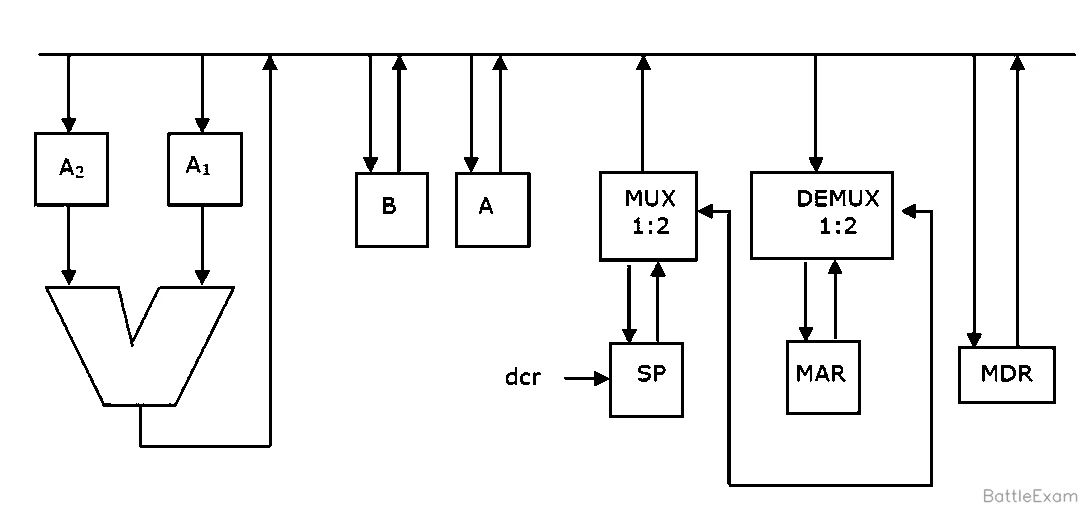
Consider the following data path of a simple non-pilelined CPU. The registers A, B, A1, A2, MDR, the bus and the ALU are 8-bit wide. SP and MAR are 16- bit registers. The MUX is of size 8x(2:1) and the DEMUX is of size 8x(1:2). Each memory operation takes 2 CPU clock cycles and uses MAR (Memory Address Register) and MDR (Memory Date Register). SP can be decremented locally. The CPU instruction "push r", where = A or B, has the specification M[SP] r SP SP - 1 How many CPU clock cycles are needed to execute the "push r" instruction ?
Arrange the following configuration for CPU in decreasing order of operating speeds: Hard wired control, Vertical microprogramming, Horizontal microprogramming.
A micro instruction is to be designed to specify: a. none or one of the three micro operations of one kind and b. none or upto six micro operations of another kind The minimum number of bits in the micro-instruction is:
A micro program control unit is required to generate a total of 25 control signals. Assume that during any micro instruction, at most two control signals are active. Minimum number of bits required in the control word to generate the required control signals will be:
Want unlimited AI-generated Alu Data Path And Control Unit questions?
Sign up free and practice with adaptive difficulty — Easy, Medium, Hard. New questions every session.
Start practising for free →