Q161JEE Main 2020NAT
The circuit shown below is working as a 8 V dc regulated voltage source. When 12 V is used as input, the power dissipated (in mW) in each diode is; (considering both zener diodes are identical) _________ .

JEE Main · Physics
Generate JEE Main level questions on Semiconductor Electronics. Focus on p-n junction, Diodes, Transistors, and Logic gates.
246 questions · 20 PYQs · 0 AI practice · JEE Main 2027
The circuit shown below is working as a 8 V dc regulated voltage source. When 12 V is used as input, the power dissipated (in mW) in each diode is; (considering both zener diodes are identical) _________ .
Which of the following will NOT be observed when a multimeter (operating in resistance measuring mode) probes connected across a component, are just reversed?
In the given circuit, value of Y is :

When a diode is forward biased, it has a voltage drop of . The safe limit of current through the diode is . If a battery of emf is used in the circuit, the value of minimum resistance to be connected in series with thediode so that the current does not exceed thesafe limit is :
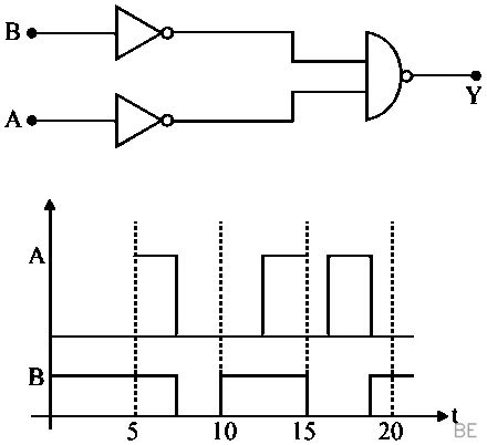
Identify the correct output signal Y in the given combination of gates (as shown) for the given inputs A and B.


The current in the network is :

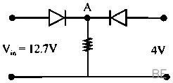
Both the diodes used in the circuit shown are assumed to be ideal and have negligible resistance when these are forward biased. Built in potential in each diode is 0.7 V. For the input voltages shown in the figure, the voltage (in Volts) at point A is ____________ .
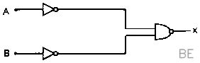
Boolean relation at the output stage-Y for the following circuit is :

Take the breakdown voltage of the zener diode used in the given circuit as . For the input voltage shown in figure below, the time variation of the output voltage is : (Graphs drawn are schematic and not to scale)


In the figure, potential difference between A and B is :

PHYSICSIdentify the operation performed by the circuit given below :

The output characteristics of a transistor is shown in the figure. When is and then value of is __________ .

With increasing biasing voltage of a photodiode, the photocurrent magnitude :
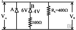
Two Zener diodes (A and B) having breakdownvoltages of and respectively, are connected as shown in athe circuit below. Theoutput voltage variation with input voltage linearly increasing with time, is given by : at ) (figures are qualitative)


In the following digital circuit, what will be the output at 'Z', when the input (A, B) are (1,0), (0,0),(1,1),(0,1):

Which of the following gives a reversible operation? [7-Jan-2020 Shift 1]


Two identical capacitors A and B, charged to the same potential 5V are connected in two different circuits as shown below at time t = 0. If the charge on capacitors A and B at time t = CR is and respectively, then (Here e is the base of natural logarithm)

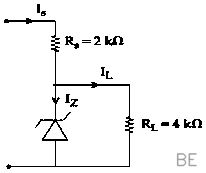
Figure shows a DC voltage regulator circuit, with a zener diode down voltage = 6V . If the unregulated input voltage varies between 10V to 16V , then what is the maximum zener current?
The logic gate equivalent to the given logic
The transfer characteristic curve of a transistor, having input and output resistance and respectively, is shown in the figure. The Voltage and Power gain, are respectively.

Want unlimited AI-generated Semiconductor Electronics questions?
Sign up free and practice with adaptive difficulty — Easy, Medium, Hard. New questions every session.
Start practising for free →