For CE transistor amplifier, the audio signal voltage across the collector resistance of is 4V. If the current amplification factor of the transistor is 100 and the base resistance is , then the input signal voltage is : [NEET 2016 P2]
NEET UG · Physics
Generate NEET level questions on Semiconductor Electronics. Focus on NCERT concepts.
150 questions · 20 PYQs · 0 AI practice · NEET UG 2027
For CE transistor amplifier, the audio signal voltage across the collector resistance of is 4V. If the current amplification factor of the transistor is 100 and the base resistance is , then the input signal voltage is : [NEET 2016 P2]
What is the output Y in the following circuit, when all the three inputs A, B, C are first 0 and then 1 ? [NEET 2016 P2]
To get output 1 for the following circuit, the correct choice for the input is : [NEET 2016 P1]
If in a p-n junction, a square input signal of V is applied as shown,then the output across will be: [NEET 2015 C]
The input signal given to a CE amplifier having a voltage gain of 150 is . The corresponding output signal will be
In the given figure, a diode is connected to an external resistance and an e.m.f. of . If the barrier potential developed across the diode is , the current in the citcuit will be
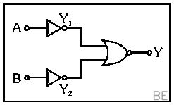
Which logic gate is represented by the following combination of logic gates ? [NEET 2015 C]
The barrier potential of a p-n junction depends on :(a) type of semi conductor material(b) amount of doping(c) temperatureWhich one of the following is correct?
The given graph represents V-I characteristic for a semiconductor device.Which of the following statement is correct?
In a n-type semiconductor, which of the following statement is true (2013 NEET)
The output (X) of the logic circuit shown in figure will be (2013 NEET)
In a common emitter (CE) amplifier having a voltage gain G, the transistor used has transconductance 0.03 mho and current gain 25. If the above transistor is replaced with another one with transconductance 0.02 mho and current gain 20, the voltage gain will be (2013 NEET)
The output from of a NAND gate is divided into two in parallel and fed to another NAND gate. The resulting gate is a (KN NEET 2013)
One way in which the operation of a transistor differs from that of a (KN NEET 2013)
In an unbiased junction, holes diffuse from the -region to -region because of (KN NEET 2013)
The figure shows a logic circuit with two inputs A and B and the output C. The voltage wave forms across A, B and C are as given. The logic circuit gate is (2012)
C and Si both have same lattice structure, having 4 bonding electrons in each. However, C is insulator whereas Si is intrinsic semiconductor. This is because (2012)
To get an output Y = 1 in given circuit, which of the following input will be correct? ABC(a)100(b)101(c)110(d)010(2012 Mains)
In a CE transistor amplifier, the audio signal voltage across the collector resistance of is 2 V. If the base resistance is and the current amplification of the transistor is 100, the input signal voltage is (2012)
The input resistance of a silicon transistor is current is changed by which results in a change in collector currently by 2 mA. This transistor is used as a common emitter amplifier with a load resistance of .The voltage gain of the amplifier is (2012 Mains)
Want unlimited AI-generated Semiconductor Electronics questions?
Sign up free and practice with adaptive difficulty — Easy, Medium, Hard. New questions every session.
Start practising for free →