In a full-wave rectifier using two ideal diodes, and are the dc and peak values of the voltage respectively across a resistive load. If PIV is the peak inverse voltage of the diode, then the appropriate relationships for this rectifier are
GATE ECE · Analog Circuits
Generate GATE-level questions on Diode Applications. Focus on: 1. Rectifiers: Half-wave, Full-wave, and Bridge rectifiers. 2. Clipping and Clamping circuits. 3. Zener diode voltage regulators.
46 questions · 6 PYQs · 0 AI practice · GATE ECE 2027
In a full-wave rectifier using two ideal diodes, and are the dc and peak values of the voltage respectively across a resistive load. If PIV is the peak inverse voltage of the diode, then the appropriate relationships for this rectifier are
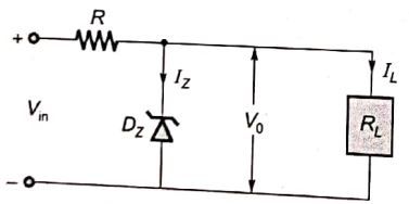
In the voltage regulator shown in the figure, the load current can vary from 100 mA to 500 mA. Assuming that the Zener diode is ideal (i.e., the Zener knee current is negligibly small and Zener resistance is zero in the breakdown region), the value of R is

The circuit shown in the figure is best described as a

The output voltage of the regulated power supply shown in the figure is

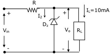
A zener diode regulator in figure is to be designed to meet the specifications: and varies from 30 V to 50 V. The zener diode has = 10V and (knee current) = 1 mA. For satisfactory opertion

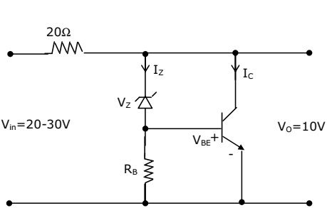
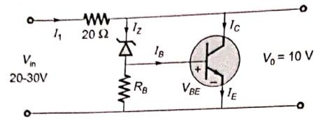
The transistor shunt regulator shown in figure has a regulated output voltage of 10 V, when the input varies from 20 V to 30 V. The relevant parameters for the Zener diode and the transistor are: =9.5, =0.3V, =99. Neglect the current through . Then the maximum power dissipated in the Zener diode ( ) and the transistor ( ) are

Want unlimited AI-generated Diode Applications questions?
Sign up free and practice with adaptive difficulty — Easy, Medium, Hard. New questions every session.
Start practising for free →